MBUS Interface
Mobile phones (especially those ones manufactured by Nokia) were one of my favorite "hobbies". Personally I thought Nokia had the best-designed phones: good hardware, smart software, leading technique. And when it came to usability Nokia was the market leader - handling a Nokia phone has always been "plug and play".
Meanwhile there are lots of dark clouds covering the blue Nokia sky ... I had some very disappointing experiences when my Communicator had to be serviced. This is not how the market leader should behave, and it's the reason I'll never ever again buy any new Nokia phone. I'll keep collecting (mainly older) phones from second hand sources (like flea markets etc.).
But now to something completely different! :-)
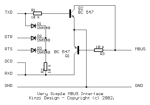
I designed a non-standard MBus interface. The common solutions use one gate of a 74HC14 for signal level adaptions (+5V / 0V at mobile side, +12V/-12V at the serial port). Since using one gate out of six is not very economic and you don't always have TTL ICs on stock at home, I just used 2 transistors.
Here's the schematic:
Please note:
If you are using this design you do this completely at your own risk! If you fry your mobile or damage it somehow else using this design I can't be held responsible.
Thank you.
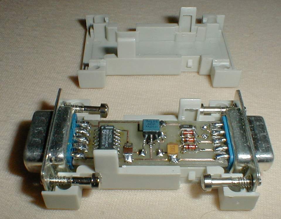
And this is my home-brewed mbus-interface using the common solution with a 74HC14 in SMD technology: